Pulsed Force Kelvin Probe Force Microscopy (PF-KPFM)
Pulsed Force Kelvin Probe Force Microscopy achieving <10nm spatial resolution for surface potential mapping.
What is Kelvin Probe Force Microscopy?
Surface potential is a physical property of materials related to their work function and the presence of surface residual charges. A popular type of SPM method for surface potential measurement is Kelvin probe force microscopy (KPFM), which was invented in the 1990s.
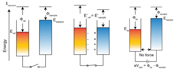
The underlying principle of KPFM is to use a DC voltage bias to compensate for the difference in surface potential to prevent electron migration upon electrical contact. KPFM has its conceptual origin in the Kelvin method, by Lord Kelvin. Consider a pair of plates of different metal types close in space: if there is an electrical connection between them, e.g., through a wire, then the Fermi level alignment occurs and electrons move from low work function metal to the high work function metal.
A net result is the emergence of charges between two metal plates, and Coulombic forces.
Pulsed Force KPFM: Our Solution
The invention of the pulsed force Kelvin probe force microscopy (PF-KPFM) is to utilize the short tip-sample distance configuration in the peak force tapping mode for surface potential measurement.
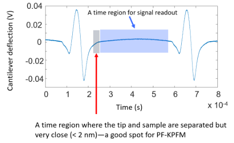
The peak force tapping mode of AFM has a deterministic contact region and detachment region. When the tip is just detached from the sample surface, the tip-sample distance is separated but still very close (< 2 nm), which is a good spot for inducing the Fermi-level alignment. The Coulombic force is mainly generated between the AFM tip apex and the sample, which is a requirement for high spatial resolution.
PFIR-KPFM: Multimodal Imaging
More characterization channels facilitate recovering the secret of nanoscale properties. The method of PFIR-KPFM is an SPM method with multimodal characterization capabilities. It integrates the method of PFIR with PF-KPFM: chemical imaging through PFIR, surface mapping through PF-KPFM, and mechanical mapping with peak force tapping, all with comparable spatial resolutions of ~10 nm in a single AFM scan.
The detailed construction of the method is described in our paper Angewandte Chemie Int. Ed., 59, 16083 (2020).
The peak force tapping mode has a characteristic trait. The resonant profile of the AFM cantilever dynamically switches between two sets: one is when the tip is detached from the sample surface; the other is when the tip is in momentary contact with the sample. The former is dominated by the cantilever free-space oscillation; the latter contains contact resonance and a shift of the free space oscillation frequency.
PFIR operates when the tip and sample are in contact; the PF-KPFM operates when they are detached. The two signal read-out channels are in parallel without interference. Integrating PFIR with PF-KPFM can be done without compromising the capability of each modality.
Application: Perovskite Materials
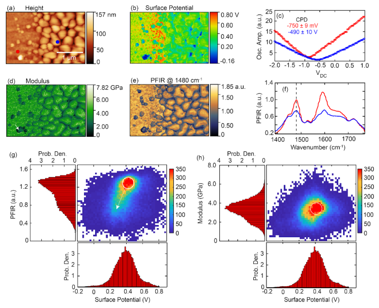
As a demonstration, we have applied PFIR-KPFM to the characterization of perovskite materials. In one AFM scan, the topography, surface potential, modulus, and PFIR @ 1480 cm⁻¹ can be obtained. PFIR Spectrum and CPD values can be obtained from the individual locations.
Correlation analysis can be obtained from simultaneously obtained image channels.
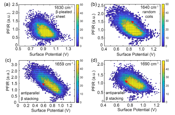
Application: Amyloid Fibrils
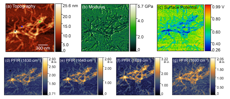
Another application of the PFIR-KPFM is on amyloid fibrils. Both surface potential and IR signals are collected. Surface potential reveals the presence of local charges; an IR signal is indicative of the secondary structures.
The correlative analysis reveals the surface potential signal with the anti-parallel beta stacking. PFIR-KPFM measurement on FapC fibrils shows a strong correlation of surface potential with antiparallel beta stacking.
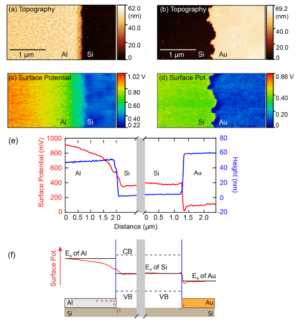
Application: Revealing Ohmic versus Schottky Junctions
The contact between Si and Al is ohmic, and the contact between Si and gold is the Schottky junction. These two types of junctions show very different surface potential distributions across the junction. Between Al and Si, the measured surface potential shows a slow envelope extending across a couple of microns, indicating a lack of barrier.
Between Si and Au, a clear barrier is observed in the surface potential, it is a manifestation of the Schottky barrier. The high spatial resolution of the PF-KPFM allows the study of these two types of barriers at a 10 nm scale under ambient conditions. For more details, please see our paper ACS Nano, 14, 4, 4839 (2020).
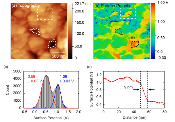
Application: Ferroelectric Surface Polarization
Another application of PF-KPFM is to reveal the surface polarization of ferroelectric materials. In this demonstration, the surface of a BaTiO₃ plate is measured, and the variation of the surface potential is observed. The variation of the surface potential is due to the adsorption of charges due to different dipole orientations.
For more details, please see our paper ACS Nano, 14, 4, 4839 (2020).
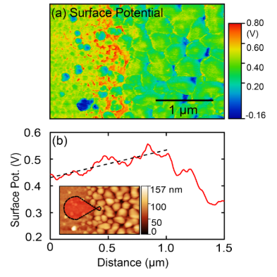
Application: Surface Charge Distribution
PF-KPFM is also useful to observe the presence of surface charge distributions. The figure shows a surface potential map of a MAPbBr₃ crystal surface with PbBr₂ degradation. Accumulation of charge appears at the MAPbBr₃ side close to the PbBr₂.
For more details, please see our paper Angewandte Chemie Int. Ed., 59, 16083 (2020).
Key Features
- <10nm spatial resolution
- Single-pass AFM scanning
- Ambient condition operation
- Work function and surface potential mapping
- PFIR-KPFM multimodal imaging capability
- Simultaneous chemical, mechanical, and electrical characterization
Applications
- Perovskite solar cell material analysis
- Amyloid fibril and protein structure studies
- Metal-semiconductor junction characterization (Ohmic vs Schottky)
- Ferroelectric material surface polarization
- Surface charge distribution mapping
- Correlative nanoscale property analysis
Key Publications
View All Related PublicationsKelvin probe force microscopy under ambient conditions
Amirhossein Zahmatkeshsaredorahi, Ruben Millan-Solsona, Devon S. Jakob, Liam Collins, and Xiaoji G. Xu
View Publication →Pulsed Force Kelvin Probe Force Microscopy—A New Type of Kelvin Probe Force Microscopy under Ambient Conditions
Amirhossein Zahmatkeshsaredorahi, Devon S. Jakob, and Xiaoji G. Xu
View Publication →